Review, teardown, and testing of LRS-150-24 Mean Well power supply
The LRS-150-24 power supply can operate from a 100–120 volt or 200–240 volt AC network. The manufacturer states it provides an output current of up to 6.5 amperes at 24 volts. The supply measures 5¾ × 3¾ × 1¼ inches (145 × 95 × 30 millimeters), made on a fiberglass printed circuit board fixed to the base's case. The top cover is perforated in a honeycomb pattern. The case and cover are both made of aluminum.
The board is put together neatly, with no visible defects. The components are arranged evenly, and soldering was done with a no-clean flux. Absolutely nothing dangles or rattles in the assembly.
No noises of any sort were noticed during the operation of the power supply.
The power supply uses a flyback circuit without PFC.
The input voltage is supplied to the input node: RF interference filter (1), a pulse surge limiter (varistor), then the voltage goes to the diode bridge (2) and two input electrolytic capacitors (3). The input voltage selector is also located here. Flyback, built on a MW03A controller (4, installed on the back side of the board) and a power switch (5) on a N-channel MOSFET transistor MMF60R290P. Unfortunately, there is no information about the controller on the Internet. The transistor has a channel resistance of 0.29 ohms at 650 volts and 13 amps. The transformer (6) is entirely covered by the casing, so it is unclear what core material is used. The output rectifier (7) is built using a Schottky diode HBR20150 in a TO-220F package screwed to the side wall and covered with casing. It is basically dual 150V 10A diodes connected in parallel. After the diode there are four output electrolytic capacitors (8) and an additional LC filter. Here (12), there is a small output voltage indicator (green LED) and a regulator (tuning resistor) for adjusting the output voltage. Input and output circuits are connected through a shared screw 7-terminal block (10). 3 terminals for the input line, neutral, and ground wires, and 2 in parallel for common and +24V output.
The main electrolytic capacitors are designed for operating temperatures up to 220°F (105°C), Rubycon. Two optocouplers (11) are installed in the feedback circuit, most likely with phototransistors transmitting control signals from the low-voltage output to the high-voltage input side.
The board has a few cutouts to increase the dielectric strength between the high-voltage and low-voltage sides of the circuit.
The picture shows that the board has three unused spots for storage output capacitors (8), most likely used in the other power supplies of the same series but with different output voltages.
Test conditions
Most tests use metering circuit #1 (see appendices) at 80°F (27°C), 70% relative humidity, and 29.8 inHg pressure.
The measurements were performed without preheating the power supply with a short-term load unless mentioned otherwise.
The following values were used to determine the load level:
Output voltage under a constant load
Power-on parameters
Powering on at 100% load
The power supply is turned off at least 5 minutes before the test, with a 100% load connected.
The oscillogram of switching to a 100% load is shown below (channel 1 is the output voltage, and channel 2 is the current consumption from the grid):
The picture shows three distinguishable phases of the power-on process:
(Turn On Delay Time) The entire process of entering the operating mode from the moment of powering on) is 119 ms.
(Output Voltage Overshoot) Output voltage overshoot is absent; the switching process is aperiodic.
Powering on at 0% load
The power supply is turned off at least 5 minutes before the test, with a 100% load connected. Then, the load is disconnected, and the power supply is switched on.
The oscillogram of switching to a 0% load is shown below:
The picture shows three distinguishable phases of the power-on process:
(Turn On Delay Time) The entire process of entering the operating mode from the moment of powering on) is 111 ms.
(Output Voltage Overshoot) Output voltage overshoot is absent; the switching process is aperiodic.
The picture shows three distinguishable phases of the power-on process:
(Turn On Delay Time) The entire process of entering the operating mode from the moment of powering on) is 111 ms.
(Output Voltage Overshoot) Output voltage overshoot is absent; the switching process is aperiodic.
Power-off parameters
The power supply was turned off at 100% load, and the input voltage was nominal at the moment of powering off. The oscillogram of the shutdown process is shown below:
The picture shows two phases of the shutdown process:
(Shut Down Hold Up Time) The supply continues to operate due to the input capacitors holding charge until the voltage across them drops to a certain critical level at which maintaining the output voltage at the nominal level becomes impossible is 31 ms.
(Output Voltage Fall Time) Reduction of the output voltage, stopping voltage conversion, and accelerating the voltage drop is 21 ms.
(Output Voltage Undershoot) Output voltage undershoot is absent, and the shutdown process is aperiodic.
Ripple voltage and current
100% load
The diagram of the current draw from the grid at 100% load is shown in the oscillogram below. The amplitude of the current is about 7.5 A:
Low-frequency output voltage ripple is under 30 mV (see the oscillogram below):
Output voltage ripple at the converter frequency is under 30 mV (see the oscillogram below):
75% load
Output voltage ripple at the converter frequency is under 30 mV (see the oscillogram below):
Low-frequency output voltage ripple is under 30 mV (see the oscillogram below):
50% load
Output voltage ripple at the converter frequency stays below 10 mV; see the oscillogram (11):

10% load
0% load
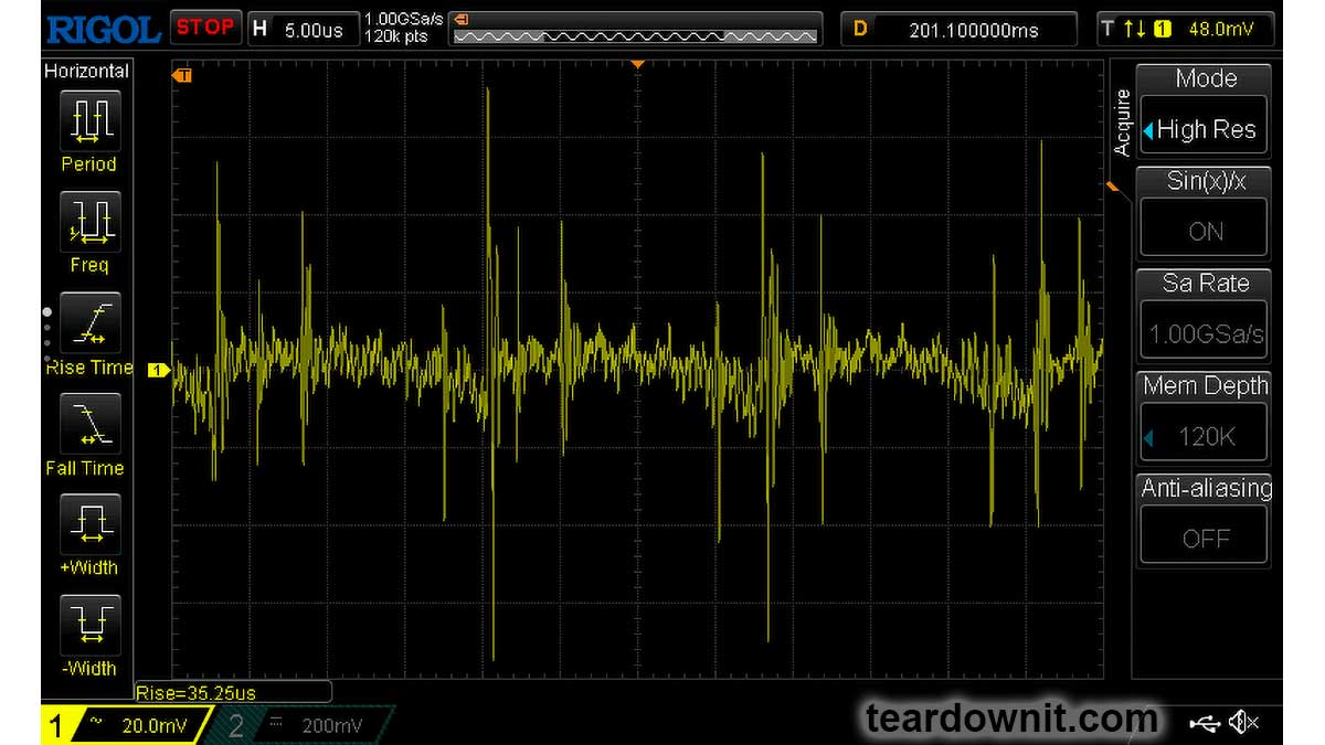
No-load current consumption was measured with a multimeter, which is 60 mA RMS.
(Power Consumption) The first assumption of excessive standby power draw of more than 7 W is wrong since the current in this mode is predominantly reactive. Indeed, the input filter in the circuit contains two capacitors with a capacitance of 0.68 μF each; these low-frequency capacitors are connected in parallel, i.e., an equivalent capacitance of 1.36 μF is connected to the input terminals. A simple calculation shows that the current through these capacitors should be equal to Ic=120×2×pi×60×1.36e-6=61.5 mA. A slight difference from the measured value can be explained by the deviation of the actual parameters from their nominal values and measurement error.
Measuring the exact active power consumption at a 0% load with a basic set of instruments (oscilloscope, multimeter, etc.) is impossible.
Output voltage ripple at the converter frequency is under 20 mV (see the oscillogram below):
The amplitude of low-frequency output voltage ripples is about 25 mV (see the oscillogram below):
Dynamic characteristics
A mode with periodic switching between 50% and 100% load was used to evaluate the dynamic characteristics. The process oscillogram is shown below (17):
It is evident that the supply’s response to loading changes is close to aperiodic, and there is no overshoot, which indicates a good stability margin. The magnitude of the response to load changes is within 200 mV.
Overload protection
The claimed protection type is "hiccup mode, recovers automatically after fault condition is removed". This was confirmed during testing. When a short circuit occurs, the power supply periodically tries to turn back on and, if the overload is still present, turns off again until the next attempt. This operating mode reduces energy losses and heating during overload. Still, it does not allow the parallel connection of multiple power supplies with a common output.
The output current for the overload protection to kick in is 8.5 A.
Input circuit safety assessment
(Input discharge) Safety assessment is based on the discharge time constant of the input circuits when disconnected from the grid; the value is 0.384 s. This means that when operating on a 120 V input voltage, the time required to discharge the input circuits to safe values (<42 V) will be 0.61 s:

Important: The result is valid for this particular power supply unit; it was obtained for testing purposes and should not be taken as a safety guarantee.
Thermal modes
When operating with no load connected, no component overheating had been noticed.
When operating under load, the input diode bridge heats up most noticeably.
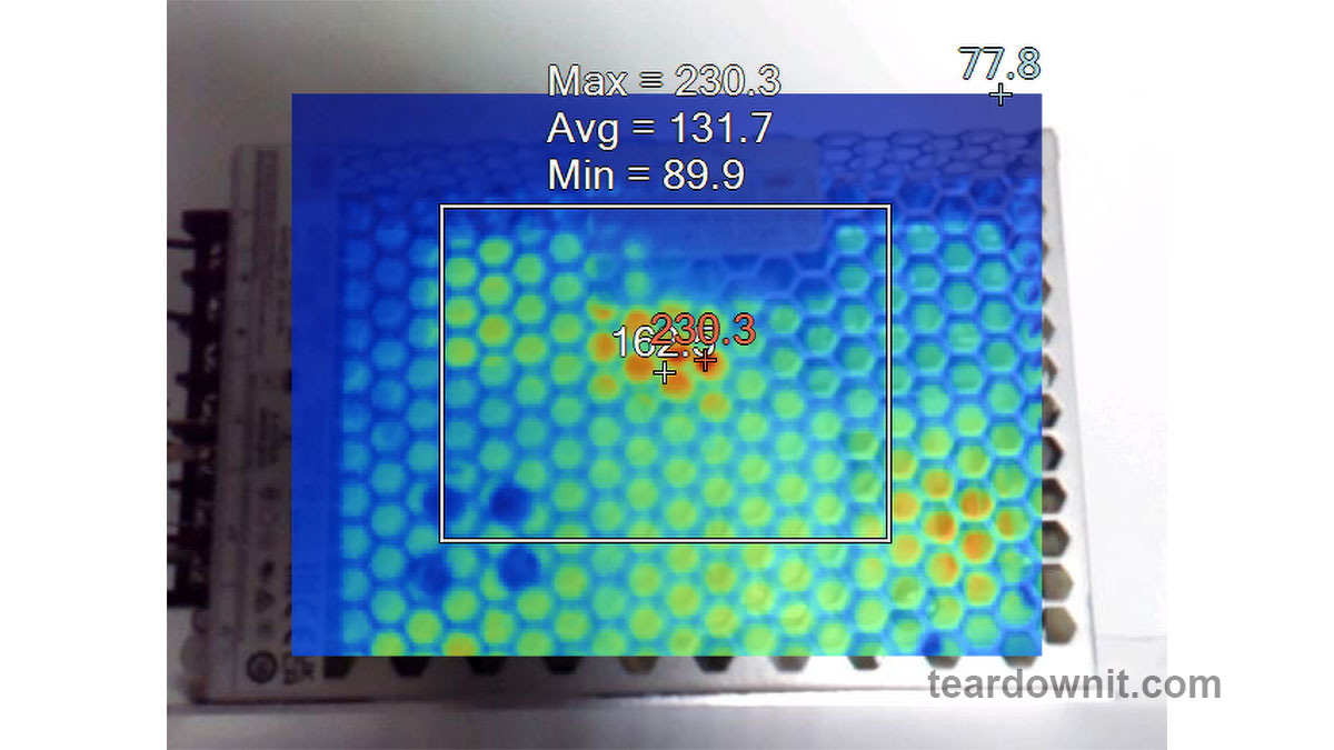
With a load of 90% and the top cover closed, the case heats up to approximately 200°F; the hottest spot is located in the area of the diode bridge rectifier.
With a load of 95% and the lid closed, the case temperature reaches 230°F:

The temperature of the bridge rectifier itself is a dangerous 250°F:
Somewhere around these load values, the power supply goes into a pulse-power-limiting mode and remains in this state either until the load drops or until it cools down. Then this 'heat up', 'limit power', 'cool down', and 'turn back on' cycle repeats.
Other things to consider:
Hot summer weather will decrease the maximum sustainable power output this supply can provide even more.
The tests were conducted with unobstructed air access to the housing for cooling; any changes may increase the heating.
This means that the power supply cannot handle its rated load for a prolonged period with no forced ventilation, and the load should be limited to 5.5 or even 5.0 A.
Conclusions
The reviewed power supply unit has characteristics generally consistent with those declared by the manufacturer, except for the long-term output power, which should be around 120 W.
The build quality is decent; no components clearly unsuitable for the general application, power draw, current, voltage, or temperature were found in the circuit.
The stability of the output voltage should be especially noted.


.jpg)
Comments
Post a Comment